

Quick Answer: Stacked microvias place successive connections above one another; staggered microvias offset those connections laterally. Stacking can solve a congested BGA escape, while staggering avoids a directly aligned sequence of microvia interfaces when space permits. Neither arrangement prevents every BGA failure: choose the route that meets the actual ball-map and electrical requirements, then qualify its material, geometry, fabrication process, and thermal exposure. Pitch alone does not make stacking mandatory, and stack height alone cannot predict production yield.
For the wider relationship between microvias, buildup layers, and routing density, see the HDI PCB guide.
Key takeaways:
- Identify whether the suspected failure is inside the board interconnect or at the BGA solder joint before changing the via architecture.
- Use stacking where it solves a demonstrated routing constraint; check whether surrounding nets can use simpler paths.
- Request qualification evidence for the proposed construction rather than accepting a generic percentage associated with a via label.
- Keep the layer-pair drawing, fabrication quotation, and test-coupon structure consistent.
Table of Contents
- 1. What’s the Real Difference Between Stacked and Staggered Microvias?
- 2. When Should You Choose Stacked Microvias?
- 3. When Are Staggered Microvias the Safer Bet?
- 4. How Many Stacked Vias Can You Reliably Use in One Stack?
- 5. What Does IPC-2226 Actually Say About Stacked vs Staggered?
- 6. How Do Aspect Ratio Rules Differ Between the Two Structures?
- 7. Which Has Better Thermal Cycling Reliability?
- 8. What Are the Cost Implications of Each Microvia Choice?
- 9. How Do You Decide for Your BGA Pitch and Layer Count?
- 10. Frequently Asked Questions (FAQ)
A layout can pass connectivity checks and still contain an interconnect that does not survive the intended assembly process. Conversely, a failed BGA connection does not establish that its microvia was responsible. This comparison focuses on choosing and checking the board’s microvia path. Package warpage, soldering defects, pad damage, and other assembly mechanisms require their own investigation.
1. What’s the Real Difference Between Stacked and Staggered Microvias?
The difference is the position of successive microvias. A stacked connection places an upper microvia over the lower connection. A staggered path moves sideways on an intermediate copper layer before continuing through another microvia. Both can connect the same starting and destination layers, but they use different pad locations and routing space.
Altium’s via-definition documentation describes stacked microvias, copper filling, and the layer pairs used to define blind, buried, and microvia structures. For a conventional stacked buildup, the supporting filled via and its prepared surface are part of the construction that must be manufactured correctly.
| Design question | Stacked path | Staggered path |
|---|---|---|
| Where are successive connections? | Vertically aligned | Laterally offset |
| What occupies the intermediate layer? | A common vertical connection area | Separate lands and a connecting copper path |
| What needs particular review? | Supporting fill, interface preparation, and registration | Offset, land clearance, connecting trace, and registration |
| Does the name establish reliability? | No; test the actual construction | No; test the actual construction |
Inspect a cross-section drawing and the plan view together. A side view may conceal a collision between staggered lands and nearby traces; a plan view may conceal which interface supports an upper stacked via. Mark every layer transition so the layout engineer and fabricator are evaluating the same electrical path.
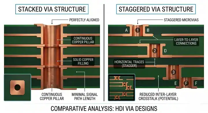
Conceptual comparison only, not to scale. Signal path length, crosstalk, and reliability depend on the actual geometry; this is not qualification evidence.
2. When Should You Choose Stacked Microvias?
Consider stacking when a trial escape shows that a lateral offset cannot fit within the available BGA fanout area while respecting the agreed manufacturing rules. A dense inner row may need a direct transition to another routing layer. That is a specific routing reason; a package-pitch threshold by itself is insufficient.
The useful inputs are the populated ball map, signal destinations, power and ground assignments, land diameters, trace width and spacing, and available routing layers. Texas Instruments’ BGA design report illustrates why active signal rows and open routing channels affect escape requirements. Its package examples are design references, not universal rules for every BGA.
As a practical review, select the most constrained signal and draw both candidate routes with manufacturing clearances included. If the staggered version collides with another land, test whether a different escape direction or destination layer resolves it. If only the stacked version meets the design requirements, record that reason beside the approved layer pair.
Mixed arrangements can be appropriate. Stacking below a congested component does not mean every nearby connection needs the same geometry. However, reducing the number of stacked sites does not automatically remove a buildup stage from the board. The remaining deepest connection may still determine the fabrication sequence and qualification requirements.
3. When Are Staggered Microvias the Safer Bet?
Staggered connections are worth evaluating when the routing area can accommodate their separate lands and lateral link. They eliminate the directly aligned arrangement at that location, which can be relevant when the concern is a weak stacked interface. This is an engineering reason to compare alternatives, not proof of a universal failure-rate advantage.
A staggered structure can still have defects in its copper connection or target interface. Registration, hole preparation, plating, laminate behavior, and the applied thermal load remain relevant. Do not treat an offset as a mechanical hinge that guarantees stress relief, or assume that an industry name such as automotive makes a particular architecture automatically compliant.
The lateral link also belongs in the electrical review. Check the reference plane, return-current transition, clearance to adjacent nets, and whether the changed route affects a sensitive signal. The via arrangement should solve the manufacturing concern without creating an unresolved routing or signal-integrity problem.
For example, during a hypothetical CAM review, a fabricator proposes offsetting two aligned microvias. Engineering should receive the revised land positions and connection path, then check clearances and electrical constraints before accepting the change. Approval should cover that drawing revision. A general note saying “stagger where possible” leaves too much uncertainty about which connections may move and who checks the consequences.
4. How Many Stacked Vias Can You Reliably Use in One Stack?
There is no universally reliable stack height or guaranteed yield associated with two, three, or more levels. The acceptable construction depends on the fabricator’s demonstrated process and the product’s qualification requirements.
What a supplier’s stack-height limit means
A supplier may recommend a two-level limit for a particular material and production process. Treat that as a capability boundary for that supplier and construction. It is useful information, but it is not an IPC-wide rule proving that all two-level stacks pass or all three-level stacks fail.
Define the count explicitly. A drawing with an L1–L2 microvia above an L2–L3 microvia contains two successive microvia levels in that path. If a buried via continues below them, show that additional structure separately. Terms such as “three-layer stack” can otherwise mean different things to purchasing and engineering.
When a construction change needs new evidence
Adding another stacked interface, changing the dielectric, or altering the supporting via structure can make previous qualification evidence less representative. Ask which of those features were present in the tested samples and which have changed in the proposed board.
IPC’s March 2019 warning discusses latent microvia failures and weak interfaces, following its 2018 white paper. It explains why conventional microsections and light microscopy alone may miss relevant defects. It does not establish a universal two-level limit or a production-yield table. Use the warning to frame the evidence request, not to invent acceptance percentages.
5. What Does IPC-2226 Actually Say About Stacked vs Staggered?
IPC-2226 HDI construction types and stacked-versus-staggered placement describe different aspects of a board. For the commonly compared Types I–III, the number of microvia buildup layers and the presence of buried vias distinguish constructions. Alignment alone does not identify the type.
| Construction | Classification distinction relevant here |
|---|---|
| Type I | One microvia layer on one or both sides of the core, without buried core vias |
| Type II | One microvia layer on one or both sides, with buried vias in the core |
| Type III | Two or more microvia layers on at least one side; successive connections may be stacked or staggered |
The AltiumLive HDI technical presentation illustrates Type II as 1-N-1 and Type III as 2-N-2 or 3-N-3. Changing a two-buildup-level path from stacked to staggered does not turn that construction into Type II.
Keep this distinction visible in the RFQ. “Type III, staggered L1–L2 and L2–L3 connections” conveys more than either “Type III” or “staggered” alone. The type does not specify every pad dimension, performance class, or required test. The companion IPC-2226 HDI types article explains how to identify and document the overall construction.
6. How Do Aspect Ratio Rules Differ Between the Two Structures?
Calculate each microvia’s aspect ratio from its depth and the agreed diameter definition. Moving a via sideways does not change that calculation. Stacked and staggered arrangements may use the same individual hole geometry while placing different demands on the connection between levels.
For a simple dimensional example, a 75 μm depth divided by a 100 μm diameter is 0.75:1. Reversing those dimensions gives approximately 1.33:1. These are geometry calculations, not predictions of fill quality or yield. State whether the dimensions describe the drilled opening, finished structure, or another agreed measurement point, because an unlabeled diameter can make two calculations appear comparable when they are not.
The microvia definition reproduced in Altium’s official documentation includes a maximum 1:1 aspect ratio and a maximum 0.25 mm structure length. The 1.33:1 example exceeds that stated ratio. A definition is not a promise that every geometry at its limit is suitable for every fabrication line. Establish the design window and tolerances with the selected fabricator.
For stacked microvias, review the via-fill selection and target surface as well as each hole’s dimensions. For staggered microvias, review the land-to-land spacing and intermediate connection. Neither a nominal 0.75:1 ratio nor a specified lateral offset replaces evidence that the proposed structure can be produced and tested successfully.
7. Which Has Better Thermal Cycling Reliability?
A meaningful comparison needs matched constructions and a defined test. A failure percentage without the sample size, thermal profile, acceptance criterion, and measurement method cannot establish which arrangement is more reliable for your board.
Assembly reflow and operating-temperature cycling
IPC-TM-650 2.6.27, Revision B addresses convection-reflow assembly simulation. It specifies at least six reflow cycles unless a deviation is agreed. For the specified resistance evaluation, the reference is the first cycle’s peak-temperature resistance; the default maximum change is 5% unless otherwise specified. These details must remain consistent with the selected revision and procurement requirements.
An operating-temperature cycling or thermal-shock program answers a different question. Its temperature range, dwell, transitions, and cycle count should relate to the intended exposure and applicable requirements. Passing assembly reflow does not by itself prove ten years of field life, and hundreds of unspecified cycles cannot be translated into a universal failure rate.
What a comparable test report must show
Request the sample drawing, material identification, via dimensions, stacked or staggered sequence, number of samples and chains, thermal conditions, measured results, and failure definition. Confirm whether the report concerns initial qualification or acceptance of the production lot being shipped.
Check the electrical data around thermal exposure, rather than relying only on a photograph of a cross-section or a room-temperature continuity result. If a report says “zero failures,” retain the denominator and test conditions when discussing it. The result describes those tested specimens; it does not establish that every future board is defect-free.
8. What Are the Cost Implications of Each Microvia Choice?
The cost difference depends on the complete fabrication sequence, geometry, inspection scope, and order. A fixed stacked-microvia premium is not a reliable substitute for comparable quotations. Likewise, there is no universal D-coupon setup price that applies across board designs and suppliers.
Ask for two quotations using the same material, outline, finished thickness, order quantity, delivery basis, and acceptance requirements. Attach the respective via maps. The comparison should state what changes: copper filling and surface preparation, sequential buildup operations, registration requirements, coupon artwork, testing, or other identified work.
| Proposed change | Question that determines its commercial effect |
|---|---|
| Offset some stacked connections | Does the manufacturing route change, or only the artwork? |
| Remove the deepest buildup connection | Can a complete buildup stage now be removed? |
| Change via diameter or dielectric | Are material, impedance, tooling, or qualification changes required? |
| Add performance testing | What sampling, reporting, and recurring lot work are included? |
Separate one-time engineering or tooling charges from recurring unit pricing. For a repeat order, also check whether the proposed lower price assumes a material substitution or a different test scope. A cheaper quotation is not automatically wrong, but its savings should be explainable without silently changing the board that engineering approved.
9. How Do You Decide for Your BGA Pitch and Layer Count?
Use pitch and layer count as design inputs, then prove the escape. The selected architecture should emerge from the actual connection paths and manufacturing limits rather than a fixed pitch-to-via table. The related guides to BGA fanout routing and HDI stackup options address those broader layout choices.
Try the critical escape paths first
Mark the active inner-row signals, reference planes, power delivery connections, and any reserved balls that the design must support. Draw the allowed microvia layer pairs and establish the pad and trace clearances. Trial-route the most constrained area before extending the same arrangement across the package.
In a hypothetical design review, a BGA’s inner signals need access to L3, while outer signals can leave on L1 or L2. Compare a directly stacked L1–L2–L3 path with a staggered route at the critical locations. If only a few paths require alignment, keep their locations explicit. This example demonstrates the review method; it does not claim a customer’s yield improvement or cost reduction.
Resolve the drawing before production
Record the accepted connection map, permitted stacked levels, supporting via construction, material stackup, and agreed qualification evidence. Have the fabricator identify any deviation before the artwork is released. If CAM changes the target layer or supporting geometry, engineering needs the revised path before accepting the change.
Return to the original failure concern. If investigation found a solder-joint defect rather than a microvia interface problem, changing the board’s via placement may not address it. Preserve the connection between the observed failure, the proposed correction, and the test that will demonstrate improvement.
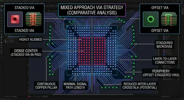
Illustrative mixed BGA escape concept, not a released layout or simulation result. Stacked center connections and staggered peripheral connections require design-specific review.
10. Frequently Asked Questions (FAQ)
Can stacked and staggered microvias coexist on one board? Yes. Define the permitted layer pairs and local arrangements in the drawing, and ensure qualification covers the structures used. A mixed layout still follows the manufacturing sequence required by its most demanding connections.
Does a 0.4 mm BGA require stacked microvias? No universal rule follows from pitch alone. The ball map, used signals, pad geometry, routing channels, and destination layers determine whether a lateral offset can fit. Evaluate the actual escape with the fabricator’s rules.
Are three stacked levels prohibited? A supplier or customer may impose that restriction, but it should be identified as a specific capability or procurement requirement. Do not substitute an unsourced industry-wide ban for a construction-specific qualification decision.
Is a cross-section enough to qualify the connection? It provides structural information, but it may not reveal a latent interface failure that appears during thermal exposure. Specify the inspection and electrical-performance evidence required for the construction and intended use.
Review Your BGA Via Layout
For a QueenEMS HDI fabrication review, send the BGA ball map, proposed stackup, via layer-pair drawing and the failure or qualification concern. Ask which connections fit the proposed manufacturing route and which require further qualification before quotation.
Written by the QueenEMS Engineering Team.
Upload your files today · Free DFM check before production · Ship worldwide
Get your PCB prototypes in as fast as 24 hours. We handle FR4, Rogers, and Flex up to 60 layers — free prototypes for 2–4 layer boards, no minimum order.
Just upload your Gerber + BOM — we source every part, assemble, and inspect (AOI + X‑Ray) so you don't have to chase suppliers. Boards ship in as fast as 24 hours.